en.radzio.dxp.pl

Lesson 9. Analog to digital converter (ADC) with Direct Memory Access (DMA)
In lesson 7 I introduce analog to digital converter, that measure voltage on one analog input. For measure voltage on more than one inputs the best way is use DMA for automatic transfer data from ADC to memory. Direct memory access is a mechanism, that allows to transfering data between memories without usage of CPU.

ADC configuration
In comparision to ADC configuration from lesson 7, we must enabled two new modes in ADC peripheral : SCAN mode and DMA mode. Scan mode allows for automatic scanning selected channels without interaction from CPU. After conversion of each channel immediatly starts new conversion of next channel in sequence. We can scan up to 16 regular channels in the sequence. In scan mode there is risk of overwrite data from previous conversion, because all conversion results are stored in this same data register (DR). For this reason in connection with SCAN mode are used DMA mode, that allows for automatic storage of conversion values in data memory after each conversion.

ADC1->CR2 = ADC_CR2_ADON | // turn on ADC
            ADC_CR2_CONT | // enable continuos mode
            ADC_CR2_DMA;   // enable DMA mode

ADC1->CR1 = ADC_CR1_SCAN;  // enable scan mode

Configuration of ADC sequencer :

ADC1->SQR1 = ADC_SEQUENCE_LENGTH(3); // four channels in sequence

ADC1->SQR3 = ADC_SEQ1(0) | // channel 0 is first in sequence
             ADC_SEQ2(1) | // channel 1 is second in sequence
             ADC_SEQ3(2) | // channel 2 is third in sequence
             ADC_SEQ4(3) ; // channel 3 is fourth in sequence

ADC1->SMPR2 = ADC_SAMPLE_TIME0(SAMPLE_TIME_239_5) | // sample time for first channel in sequence
              ADC_SAMPLE_TIME1(SAMPLE_TIME_239_5) | // sample time for second channel in sequence
              ADC_SAMPLE_TIME2(SAMPLE_TIME_239_5) | // sample time for third channel in sequence
              ADC_SAMPLE_TIME3(SAMPLE_TIME_239_5) ; // sample time for fourth channel in sequence

Variable for storing conversion values :

vu16 AIN[4]; // 4 locations

DMA configuration
Before we use DMA for transferring data between two areas of memory space of STM32 microcontroller, we have to say to DMA peripheral some informations, like as : source address (data register of ADC), destination address (table for conversions results), number of transfers (amount of scanned input channels).

DMA1_Channel1->CPAR  = (uint32_t)(&(ADC1->DR)); // peripheral (source) address
DMA1_Channel1->CMAR  = (uint32_t)AIN;           // memory (desination) address
DMA1_Channel1->CNDTR = 4;                       // 4 transfers

DMA1_Channel1->CCR |= DMA_CCR1_CIRC |    // circular mode enable
                      DMA_CCR1_MINC |    // memory increment mode enable
                      DMA_CCR1_MSIZE_0 | // memory size 16 bits
                      DMA_CCR1_PSIZE_0;  // peripheral size 16 bits

DMA1_Channel1->CCR |= DMA_CCR1_EN ; // Enable channel

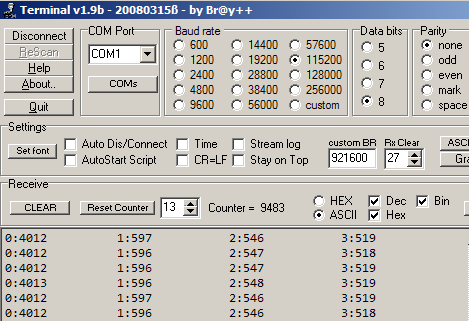
Sending conversion results
For sending result we use code from lesson 8.

do{
  sprintf(str, "0:%d\t\t1:%d\t\t2:%d\t\t3:%d\r", AIN[0], AIN[1], AIN[2], AIN[3]);
  USART_PutString(str);
  for(dly = 0; dly < 1000000; dly++);
}while(1);

Complete source code :

//=============================================================================
// STM32VLDISCOVERY tutorial
// Lesson 9. Analog to digital converter (ADC) with direct memory access (DMA)
// Copyright : Radoslaw Kwiecien
// http://en.radzio.dxp.pl
// e-mail : radek(at)dxp.pl
//=============================================================================
#include "stm32f10x.h"
#include "antilib_gpio.h"
#include "antilib_adc.h"
//=============================================================================
// Defines
//=============================================================================
#define USART_RX_GPIO GPIOA
#define USART_RX_PIN 10

#define USART_TX_GPIO GPIOA
#define USART_TX_PIN 9
//=============================================================================
// Send single char
//=============================================================================
void USART_PutChar(uint8_t ch)
{
  while(!(USART1->SR & USART_SR_TXE));
  USART1->DR = ch;
}
//=============================================================================
// Send text
//=============================================================================
void USART_PutString(uint8_t * str)
{
while(*str != 0)
  {
  USART_PutChar(*str);
  str++;
  }
}
//=============================================================================
// Global variables
//=============================================================================
vu16 AIN[4];  // table for conversions results
char str[32]; // buffer for text
//=============================================================================
// main function
//=============================================================================
int main(void)
{
vu32 dly;
RCC->APB2ENR |= RCC_APB2ENR_IOPAEN | RCC_APB2ENR_IOPCEN | RCC_APB2ENR_AFIOEN | RCC_APB2ENR_ADC1EN | RCC_APB2ENR_USART1EN;
RCC->AHBENR |= RCC_AHBENR_DMA1EN;

#if (USART_RX_PIN > 7)
USART_RX_GPIO->CRH = (USART_RX_GPIO->CRH & CONFMASKH(USART_RX_PIN)) | GPIOPINCONFH(USART_RX_PIN, GPIOCONF(GPIO_MODE_INPUT, GPIO_CNF_INPUT_PULLUPDOWN));
#else
USART_RX_GPIO->CRL = (USART_RX_GPIO->CRL & CONFMASKL(USART_RX_PIN)) | GPIOPINCONFL(USART_RX_PIN, GPIOCONF(GPIO_MODE_INPUT, GPIO_CNF_INPUT_PULLUPDOWN));
#endif

#if (USART_TX_PIN > 7)
USART_TX_GPIO->CRH = (USART_TX_GPIO->CRH & CONFMASKH(USART_TX_PIN)) | GPIOPINCONFH(USART_TX_PIN, GPIOCONF(GPIO_MODE_OUTPUT2MHz, GPIO_CNF_AFIO_PUSHPULL));
#else
USART_TX_GPIO->CRL = (USART_TX_GPIO->CRL & CONFMASKL(USART_TX_PIN)) | GPIOPINCONFL(USART_TX_PIN, GPIOCONF(GPIO_MODE_OUTPUT2MHz, GPIO_CNF_AFIO_PUSHPULL));
#endif

GPIOA->CRL = (GPIOA->CRL & 0xFFFF0000) |
             GPIOPINCONFL(0, GPIOCONF(GPIO_MODE_INPUT, GPIO_CNF_INPUT_ANALOG)) |
             GPIOPINCONFL(1, GPIOCONF(GPIO_MODE_INPUT, GPIO_CNF_INPUT_ANALOG)) |
             GPIOPINCONFL(2, GPIOCONF(GPIO_MODE_INPUT, GPIO_CNF_INPUT_ANALOG)) |
             GPIOPINCONFL(3, GPIOCONF(GPIO_MODE_INPUT, GPIO_CNF_INPUT_ANALOG));

ADC1->CR2 = ADC_CR2_ADON | // turn on ADC
            ADC_CR2_CONT | // enable continuos mode
            ADC_CR2_DMA;   // enable DMA mode

ADC1->CR1 = ADC_CR1_SCAN; // enable scan mode

ADC1->SQR1 = ADC_SEQUENCE_LENGTH(3); // four channels in sequence

ADC1->SQR3 = ADC_SEQ1(0) | // channel 0 is first in sequence
             ADC_SEQ2(1) | // channel 1 is second in sequence
             ADC_SEQ3(2) | // channel 2 is third in sequence
             ADC_SEQ4(3) ; // channel 3 is fourth in sequence

ADC1->SMPR2 = ADC_SAMPLE_TIME0(SAMPLE_TIME_239_5) | // sample time for first channel in sequence
              ADC_SAMPLE_TIME1(SAMPLE_TIME_239_5) | // sample time for second channel in sequence
              ADC_SAMPLE_TIME2(SAMPLE_TIME_239_5) | // sample time for third channel in sequence
              ADC_SAMPLE_TIME3(SAMPLE_TIME_239_5) ; // sample time for fourth channel in sequence

DMA1_Channel1->CPAR  = (uint32_t)(&(ADC1->DR)); // peripheral (source) address
DMA1_Channel1->CMAR  = (uint32_t)AIN; // memory (desination) address
DMA1_Channel1->CNDTR = 4; // 4 transfers

DMA1_Channel1->CCR |= DMA_CCR1_CIRC |    // circular mode enable
                      DMA_CCR1_MINC |    // memory increment mode enable
                      DMA_CCR1_MSIZE_0 | // memory size 16 bits
                      DMA_CCR1_PSIZE_0;  // peripheral size 16 bits

DMA1_Channel1->CCR |= DMA_CCR1_EN ; // Enable channel

ADC1->CR2 |= ADC_CR2_ADON; // Turn on conversion

USART1->CR1 = USART_CR1_UE | USART_CR1_TE;
USART1->BRR = (SystemCoreClock / 115200);

USART_PutString("STM32VLDISCOVERY tutorial lesson 9\r");

do{
  sprintf(str, "0:%d\t\t1:%d\t\t2:%d\t\t3:%d\r", AIN[0], AIN[1], AIN[2], AIN[3]);
  USART_PutString(str);
  for(dly = 0; dly < 1000000; dly++);
}while(1);

}
//=============================================================================
// End of file
//=============================================================================

Results on terminal :

adc dma


(c) Radosław Kwiecień